PS3 六向手把可以在 Windows 下使用了。
http://forums.ps2dev.org/viewtopic.php?t=7099
12/07/2006
PS3 入手
今天終於入手 PS3 了,想了這麼久,
在光華商場裡的印地安小賣店買的,
真是高興啊~
雖然要綁2片遊戲和另一隻手把,總共 23230 元。
但總算滿足了一下這半年多的心勞。
遊戲 1 - 鋼彈
遊戲 2 - RR7
主機 60 G 版本,聲音真的很小,真是美啊!MSD Duo 也不會卡住。
目前正在安裝 Fedora Core 6 PPC 中。
看來唯一的缺憾就是目前只是用 PS3 輸出到我的電視卡中,誰叫我沒
電視咧!用 480i 輸出,真是太浪費啦!不過好處是一個螢幕就搞定,
也許將來買張有支援 1080P 的電視卡也可以”暫時”取代那超貴的 LCD-TV。
SONY 對 PS3 Linux 的支援可真不小。
CELL-Linux-CL_20061110-ADDON 這張 CD 裡有比較完整的資訊,目前
看來 Kernel 都是架在 Hypervisor 之上,難怪我安裝 FC6 這麼慢。
12/05/2006
Plugin 的 Open Source
不只是說怎麼寫 Plugin ,而是怎麼替自己的程式建立一個能夠 Load Plugin 的介面。
參考資料
http://www.linux-ha.org/_cache/TechnicalPapers__pils.pdf
CVS Code:
http://cvs.linux-ha.org/viewcvs//viewcvs.cgi/linux-ha/lib/pils/
參考資料
http://www.linux-ha.org/_cache/TechnicalPapers__pils.pdf
CVS Code:
http://cvs.linux-ha.org/viewcvs//viewcvs.cgi/linux-ha/lib/pils/
FlashPlayer 之加速 2
1. OnTimer() -> UpdateScreen() -> DrawScreen()
2. SYSFONT 會減慢速度,因為每次 UpdateRect() 都會 TestDeviceFont()。
3. DISABLE_FOCUS_RECT 在 UpdateRect() 中,若取消可加速,但應該不多,只是少個判斷式。
4. 關於 Mouse Cursor 的相關函數都可以取消以加快速度,目前反正沒 Mouse。
另外應呼叫 BlinkCursor() 來更新 Cursor。
2. SYSFONT 會減慢速度,因為每次 UpdateRect() 都會 TestDeviceFont()。
3. DISABLE_FOCUS_RECT 在 UpdateRect() 中,若取消可加速,但應該不多,只是少個判斷式。
4. 關於 Mouse Cursor 的相關函數都可以取消以加快速度,目前反正沒 Mouse。
另外應呼叫 BlinkCursor() 來更新 Cursor。
FlashPlayer - raster 對速度影響
在做一些 Flash 動畫效果時發現了一個有趣的現象,
即使兩個變動的區塊 (Rect) 大小相同,但寬形的區塊
會比長形的區塊要快,我想是因為 FlashPlayer 是以 raster
方式來做運算的,較多的 raster (長形) 處理會較慢。
這點倒是可以加入最佳化的考量中。
(當然,在快速的機器中是很難發現這個結果的。)
另外也想到了一個重點,也許重新對 data 處理 alignment 可
以加速單一指令運算的速度。目前尚未看到 FlashPlayer 程式
中有對 alignment 處理。但對支援 SIMD 的機器倒是有做 Assembly
Level 的最佳化。
關於 Glibc malloc 的 alignment 可以參考這。
http://www.delorie.com/gnu/docs/glibc/libc_31.html
12/02/2006
Track+ : 專案管理系統
Track and Manage Issues
- Easy and pleasant to use
- Clean and well organized user interface
- Fully web based, no client installation
- Highly configurable
- Email reminders for due tasks
- Overview diagrams
- Budgets and expenses (new!)
- Nice template based PDF reports
- Easy to setup and administer
- Powerful access control
- Manages hundreds of projects
- More features...
http://www.trackplus.com/
OProfile - Open Source Profiler
OProfile is a system-wide profiler for Linux systems, capable of profiling all running code at low overhead. OProfile is released under the GNU GPL.
It consists of a kernel driver and a daemon for collecting sample data, and several post-profiling tools for turning data into information.
OProfile leverages the hardware performance counters of the CPU to enable profiling of a wide variety of interesting statistics, which can also be used for basic time-spent profiling. All code is profiled: hardware and software interrupt handlers, kernel modules, the kernel, shared libraries, and applications.
http://oprofile.sourceforge.net/
IDEA - 加速 FlashPlayer 的一些方式
IDEA - 加速 FlashPlayer 的一些方式
- IXP425 也有 CP0 具有 SIMD 能力,應該可以用來做 Assembly Level 的加速。
(RGBI -> RGBIL) - 應該加速的對象:
- CompositeRGB()
- CompositeRGBSolid()
- DrawSolidSlab32()
- DrawRGBSlab32A()
- CompositeSolidSlab()
- CompositeGradientSlab()
- CompositeBitmapSlab()
- GetBackground32()
- GetBackgroundWhite()
- Blt32toI()
- Blt32to32() - 也許應該 disable SMOOTHBITS
- 使用 -O2 來 Compile
- Intel Xscale 微架構代碼優化建議
- Data Access Performance Optimization on the Intel® 80321 I/O Processor
- Intel XScale IOP Linux
- GCC Assembler Instructions with C Expression Operands
- GCC-Inline-Assembly-HOWTO
- Intel® XScale™ Microarchitecture Assembly Language Quick Reference Card (pdf)
CBEA Note - 07
7. MFC Commands
7.1.1 Defined Commands
- MFC commands can either be issued by code running on the SPU, or by code running on another processor or device, such as the PPE.
- SPU executes a series of channel instructions to issue an MFC command.
- other processors or devices performs a series of memory-mapped I/O (MMIO) transfers to issue an MFC command to an SPE.
- The commands issued are queued to one of these command queues of the MFC:
• MFC proxy command queue for any MMIO-initiated commands
• MFC SPU command queue for any channel-initiated commands - MFC commands that transfer data are referred to as MFC DMA commands.
- Transfer data into an SPE (from main storage to local storage) are considered get commands.
- Transfer data out of an SPE (from local storage to main storage) are considered put
commands.
- Commands can be categorized into three classes, as follows:
• Defined
• Illegal
• Reserved
7.1.1 Defined Commands
- Defined commands fall into one of three categories:
• Data transfer commands
– Data moved from local storage and placed in main storage (put commands)
– Data moved into local storage from main storage (get commands)
• SL1 cache-management commands
• Synchronization commands
- Unaligned DMAs are not supported by the CBEA.
- If an unaligned DMA operation is encountered, the MFC command queue processing is suspended and an DMA alignment interrupt is generated.
- Commands with a suffix of “l” use list elements located in the local storage pointed to by the DMA list local storage address (LA) parameter of a list command.
- The element contains the lower order word of the effective address (LEAL) and the transfer size (LTS).
- The DMA list commands use a list of effective addresses and transfer size pairs, or list elements, stored in local storage as the parameters for the DMA transfer. These parameters are used for SPU-initiated DMA list commands, which are not supported on the MFC proxy command queue.
12/01/2006
CBEA Note - 06
6. Memory Flow Controller

• MMIO interface
• MFC registers
• DMA controller
6.1 MFC Facilities
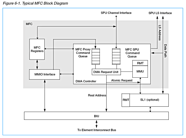
- In a CBEA-compliant processor, the MFC serves as an interface to the system and to other elements for an SPU.
- It provides the primary mechanism for data transfer, protection, and synchronization between main storage and the local storage arrays.
- there is logically an MFC for each SPU in a processor.
- MFC has two interfaces to the SPU, two interfaces to the Bus Interface Unit (BIU), and two interfaces to an optional SL1 cache.
- SPU channel interface allows the SPU to access MFC facilities and to issue MFC commands.
- SPU local storage interfaces is used by the MFC to access the local storage in the SPU.
- One interface to the BIU allows memory-mapped I/O (MMIO) access to the MFC facilities. This interface also allows other processors to issue MFC
commands. Commands issued using MMIO are referred to as MFC proxy commands. - The other interface to the BIU carries the real address.
- The interfaces to the SL1 cache are mainly for data transfers.
- One interface is used by the MFC for access to the address translation tables in main storage and the other interface of the SL1 cache is used for the transfer of data between main storage and local storage.
• MMIO interface
• MFC registers
• DMA controller
- The MMIO interface maps the MFC facilities of the SPU into the real address space of the system. (allows access to the MFC facilities from any processor, or any device in the system.)
- MMIO interface can be configured to map the local storage of the SPU into the real address space. (map local storage to real address space)
- allows direct access to the local storage from any processor or any device in the system
- enabling local-store-to local-store transfers
- ability for I/O devices to directly access the local storage domain - Coherency is not maintained between SPU and MMIO accesses of the local storage domain.
6.1 MFC Facilities
- Most of the MFC facilities are contained in the MFC Registers unit.
- Some facilities are contained in the Direct Memory Access Controller (DMAC).
- The facilities within the MFC:
User mode environment facilities include:
• Mailbox Facility (see page 90)
• SPU Signal Notification Facility (see page 94)
• Proxy Tag-Group Completion Facility (see page 82)
• MFC Multisource Synchronization Facility (see page 96)
• SPU Control and Status Facilities (see page 86)
• SPU Isolation Facility (see page 163)
Privileged mode environment facilities include:
• MFC Privileged Facilities (see page 197)
– MFC State Register One (see page 197)
– MFC Logical Partition ID Register (see page 199)
– MFC Storage Description Register (see page 200)
– MFC Data Address Register (see page 201)
– MFC Data Storage Interrupt Status Register (see page 202)
– MFC Address Compare Control Register (see page 203)
– MFC Local Storage Address Compare Facility (see page 205)
– MFC Command Error Register (see page 207)
– MFC Data Storage Interrupt Pointer Register (see page 208)
– MFC Control Register (see page 209)
– MFC Atomic Flush Register (see page 212)
– SPU Outbound Interrupt Mailbox Register (see page 213)
• SPU Privileged Facilities (see page 215)
– SPU Privileged Control Register (see page 215)
– SPU Local Storage Limit Register (see page 217)
– SPU Configuration Register (see page 221)
• SPE Context Save and Restore (see page 223) - The SPEs and PPE instruct the MFC to perform these DMA operations by queuing DMA command requests to the MFC through one of the command queues:
• Commands issued by an SPE are queued to the MFC SPU command queue
• Commands issued by a PPE are queued to the MFC proxy command queue - The MFC uses a MMU to perform all MFC address translations and MFC access protection checks required for the DMA transfers.
- The MMU handles MFC transfers in much the same way that the PPE storage addressing facility handles load-and-store operations.
CBEA Note - 05
5. Synergistic Processor Unit
- The intent of the SPU is to fill a void between general-purpose processors and special-purpose hardware.
- SPU aims to achieve leadership performance on critical workloads for game, media, and broadband systems.
- The intent of the SPU and the CBEA is to provide a high degree of control to expert (real-time) programmers while maintaining ease of programming.
- The SPU implements a new instruction set architecture (ISA).
- The main characteristics of this architecture are:
• Load-and-store architecture with sequential semantics, using a set of 128 registers, each of which is 128 bits wide.
• Single-instruction, multiple-data (SIMD) capability
– Sixteen 8-bit integers
– Eight 16-bit integers
– Four 32-bit integer or four single-precision floating-point values
– Two double-precision floating point
• Load-and-store access to an associated local storage.
• Channel input/output for MFC control (used for external data access). - The SPU has the following restrictions:
• No direct access to main storage (access to main storage using MFC facilities only)
• No distinction between user mode and privileged state
• No access to critical system control such as page-table entries (this restriction should be enforced by PPE privileged software).
• No synchronization facilities for shared local storage access - The intent of the SPU is to enable applications that require a high computational unit density.
CBEA Note - 04
4. PowerPC Processor Element
4.1 PowerPC Architecture Book I and Book II Compatibility
The PPE provides binary compatibility for PowerPC applications, except as described in Section 4.1.2 Incompatibilities with PowerPC Architecture, Book I on page 39.
4.1.1 Optional Features in PowerPC Architecture, Book I (Required for CBEA)
4.1.3 Optional Features in PowerPC Architecture, Book II (Required for CBEA)
4.1.4 Incompatibilities with PowerPC Architecture, Book II
4.1.5 Extensions to the PowerPC Architecture
- The CBEA includes a PowerPC processor, which, with the MFC is known as the PowerPC Processor Element (PPE).
- The PPE must be a 64-bit implementation, all effective addresses and registers, except some special-purpose and memory-mapped I/O (MMIO) registers are 64 bits long.
- All implementations have two modes of operation: 64-bit mode and 32-bit mode.
- All instructions are available in both modes.
- The CBEA does not permit a PPE implementation that provides only the equivalent of 32-bit mode.
4.1 PowerPC Architecture Book I and Book II Compatibility
The PPE provides binary compatibility for PowerPC applications, except as described in Section 4.1.2 Incompatibilities with PowerPC Architecture, Book I on page 39.
4.1.1 Optional Features in PowerPC Architecture, Book I (Required for CBEA)
- The following facilities and instructions are considered optional in the PowerPC Architecture, but are required for the PPE by the CBEA user mode environment.
• Floating reciprocal estimate single A-form (fres)
• Floating reciprocal square-root estimate A-form (frsqte)
• Vector/SIMD multimedia extension
- Currently there are no incompatibilities with PowerPC Architecture, Book I.
4.1.3 Optional Features in PowerPC Architecture, Book II (Required for CBEA)
- The following facilities and instructions are considered optional in the PowerPC Architecture, but are required in the CBEA.
• Data cache block touch X-form (dcbt)
This is an optional version of dcbt that permits a program to provide a hint that a sequence of data cache blocks is likely to be needed soon.
4.1.4 Incompatibilities with PowerPC Architecture, Book II
- Currently there are no incompatibilities with PowerPC Architecture, Book II.
4.1.5 Extensions to the PowerPC Architecture
- For information on extensions in the CBEA to the PowerPC Architecture, see Appendix E .
11/29/2006
CBEA Note - 03
Chapter 3. Storage Models
The CBEA-compliant processor implements two concurrent storage models for an application program:
3.2 SPU Local Storage Model
3.3 Single-Copy Atomicity
3.6 Storage Control Attributes
The CBEA-compliant processor implements two concurrent storage models for an application program:
- virtual storage model of the PPE (also used by MFCs for DMA operations) . The PPE virtual storage model allows privileged software to provide different views of the real memory
and I/O devices for the PPE and any MFC unit DMA transfers. It is possible for multiple virtual address spaces to exist. - local storage model of the SPU. The SPU local storage model is restricted to applications running on SPUs and data transfers handled by the MFC.
- Allows applications to exist within a virtual address space larger than either the effective address space or the real address space.
- In a typical CBEA-compliant processor system, the effective address space of each program is a subset of a larger virtual address space managed by privileged software.
- The privileged software manages the real storage resources of the system by setting up the tables and other information used by the hardware address translation facility.
- Access to the virtual pages can be read/write, read only, or no access.
〔
基本上記憶體管理模型還是用 segmentation 加上 paging,只是與 x86 用詞上不太一樣:

CBEA 架構下是:

             segmentation                   paging
virtual address -----------> effective address -----> real address

x86 架構下則是:

             segmentation                paging
logical address -----------> linear address -----> physical address
〕
3.2 SPU Local Storage Model
- Each SPU has its own dedicated area of local storage.
- The individual local storage areas can be aliased to a real address within the main storage
domain and any PPE can access these areas by using the appropriate effective address.
- The CBEA allows the local storage of an SPU to have an alias in the real address space in the main storage domain.
- This allows other processors in the main storage domain to access local storage through appropriately mapped effective address space.
- Privileged software should access the aliased pages of local storage in the main storage domain.
- If not accessed as caching inhibited, software must explicitly manage the coherency of local storage with other system caches.
〔若不以 cache inhibited 方式來存取 local storage,就必須由程式自己來處理 cache 與真正 local storage 間同步的問題了。〕
- MFC commands, which access an effective address range that maps to its own local storage can produce an error or unpredictable results.
〔 MFC command 若存取了對應到自己的 local storage 範圍時,則會產生錯誤會或不可預期的結果。因為此時 DMA 的來源與目的區塊是重疊的。〕 - Therefore, it is the programmer's and privileged software's responsibility to avoid an unintended overlap, which can result in the corruption of data.
3.3 Single-Copy Atomicity
- In the PowerPC Architecture, the following single register accesses are always atomic:
• Byte accesses (all bytes are aligned on byte boundaries)
• Halfword accesses aligned on halfword boundaries
• Word accesses aligned on word boundaries
• Doubleword accesses aligned on doubleword boundaries
• Quadword accesses aligned on quadword boundaries - Only quadword accesses of local storage are atomic.
〔沒有 alignment 的存取也不是 atomic 的,而在存取 local storage 時,只有 quadword access 是 atomic〕
- Harvard-style cache of PPC.
- A location in the data cache is considered to be modified in that cache if the location has been modified (for example, by a store instruction) and the modified data has not been written to main storage.
- Cache management instructions allow programs to manage the caches when needed.
- The Cache Management Instructions allow programs to:
• Invalidate the copy of storage in an instruction cache block (icbi)
[invalid an instruction cache]
• Provide a hint that the program will probably soon access a specified data cache block (dcbt, dcbtst)
[set a cache hint]
• Set the contents of a data cache block to zeros (dcbz)
[clear cache]
• Copy the contents of a modified data cache block to main storage (dcbst)
[copy back]
• Copy the contents of a modified data cache block to main storage and make the copy of the block in the data cache invalid (dcbf)
[copy back and set invalid] - The SL1 data cache commands allow programs to:
• Bring a range of effective addresses into the SL1 (sdcrt)
• Bring a range of effective addresses into the SL1 (sdcrtst)
• Write zeros to the contents of a range of effective addresses (sdcrz)
• Store the modified contents of a range of effective addresses (sdcrst)
• Store the modified contents of a range of effective addresses and invalidate the block (sdcrf) - Above instructions are treated as no operations (no-op) instructions in implementations without an SL1.
- 當一連串的存取同一個位址的 memory 時,並不能保證每次的 store 都會真的寫入到這個位址上,因為 cache 的關係,所以軟體必須要自己來控制 Memory coherence 的問題。
(原文寫了很多,就是要說明這一點啦~)
3.6 Storage Control Attributes
- Storage control attributes are associated with units of storage that are multiples of the page size.
〔以 page 為單位的 storage control attributes〕 - The storage control attributes are:
• Write through Required
〔從 cache 寫到了真的記憶體位址中〕
• Caching Inhibited
〔不使用 cache 〕
• Memory Coherence Required
〔需要 Memory Coherence〕
• Guarded
- The CBEA supports the sharing of storage between programs, between different instances of the same program, between SPUs, and between processors and other devices.
- It also supports access to a storage location by one or more programs using different effective addresses or DMA addresses.
〔segmentation + paging 吧〕 - Storage is shared in blocks of an integral number of pages.
- When the same storage location has different effective addresses, the addresses are called aliases.
- Each application can be granted separate access privileges to aliased pages.
CBEA Note - 02
Part 2 User Mode Environment
Chapter 2
2.1 Instruction and Command Classes
2.1.1 Defined Class
2.1.2 Illegal Class
2.1.3 Reserved Class
2.2 Forms of Defined Instructions and Commands
In the defined set of instructions and commands, certain field or parameter settings can execute more efficiently, or can produce an error condition. The CBEA defines the field and parameter settings as preferred forms or invalid forms.
2.2.1 Preferred Forms
2.2.2 Invalid Forms
2.2.3 Optional Forms
2.2.4 Optional Fields
2.3 Exceptions
2.4 SPU Events
The SPU supports an event facility that provides the capability to
〔嗯嗯~原來 SPU interrupt handler 在 LS address '0' 啊。〕
Chapter 2
2.1 Instruction and Command Classes
- Both the PPE and the SPU components execute programs that consist of instructions that specify the type of actions they are to perform.
〔PPE 與 SPU 需指定 type of actions〕 - The MFCs execute commands that specify the type of data copying or movement
they are to perform.
〔MFC command 則需指定 type of data〕 - These instructions and commands can be categorized into three classes, as follows:
• Defined Class (see page 28)
• Illegal Class (see page 28)
• Reserved Class (see page 29) - The class of an instruction or command is determined by examining the opcode.
〔指令的類別由 opcode 來決定〕 - If an instruction opcode, or a combination of opcode and extended opcode, is not that of a defined or reserved instruction, then the instruction is illegal.
〔不符合型態的指令會被認定為非法指令。〕 - In future versions of the CBEA, instructions or commands that are currently illegal can become defined (by being added to the architecture), or reserved (by being assigned to a special-purpose operation). Similarly, some instructions or commands that are currently reserved can become defined in a subsequent architecture release.
〔非法指令的判定標準在未來版本的 CBEA 裡是會變動的。〕
2.1.1 Defined Class
- Defined instructions and commands are guaranteed to be provided in all implementations. The only deviations permitted are instructions or commands specifically identified in their descriptions as optional.
〔屬於 Defined 類別中的指令或命令在未來也被保證能夠在所有的 CBEA implementation 中繼續執行。會變動的只有 optional 的部分。〕 - Defined instructions or commands can have preferred forms, or invalid forms, or both. These forms are also indicated in the relevant description.
〔已定義的指令或命令有 preferred 格式或 invalid 格式,或是兩種格式兼具。格式會在相關的敘述中說明。〕
2.1.2 Illegal Class
- Any attempt to execute an illegal PPE instruction causes an exception interrupt, but has no other effect on the PPE operation.
〔非法的 PPE 指令將導致一個 interrupt,但不影響此 PPE opertaion。〕 - Any SPU that encounters an illegal instruction immediately halts program execution, records the event in its status register, and requests an external interrupt.
〔SPU 一旦執行到非法的指令將會停止執行整個程式,並把此事件紀錄在 status register中,最後產生一個 external interrupt。〕 - The illegal-instruction interrupt should be enabled and routed to a PPE. In either case, the exception interrupt should cause the illegal-instruction handler for the system to be invoked, which then takes appropriate action.
〔非法指令產生的 interrupt 都應被導向 PPE ,由 illegal-instruction handler 來處理。〕
2.1.3 Reserved Class
- Reserved instructions are allocated to specific purposes outside the scope of the CBEA, or
are intended for use in future extensions of the CBEA.
〔Reserved instructions 是超出 CBEA 定義之外,但未來有可能被 CBEA 的 extensions 所使用的指令集。〕 - These are the only commands that should be used by implementation-dependent applications.
〔這一種類的指令集應只被 implementation-dependent application 所使用。〕
2.2 Forms of Defined Instructions and Commands
In the defined set of instructions and commands, certain field or parameter settings can execute more efficiently, or can produce an error condition. The CBEA defines the field and parameter settings as preferred forms or invalid forms.
2.2.1 Preferred Forms
- Some defined instructions and commands have preferred forms. The preferred form of an instruction or command executes in an efficient manner; any other form can take significantly longer to execute.
〔一些已定義的指令集有 preferred 格式,以此種格式被執行時會有較佳的效率。〕
2.2.2 Invalid Forms
- Some defined instructions and commands have invalid forms.
〔一些 Defined instructions and commands 則有無效的格式。〕
2.2.3 Optional Forms
- Some of the defined instructions are optional. Any attempt to execute an optional instruction that is not provided by the implementation causes the system illegal-instruction interrupt handler to be invoked.
- Currently, there are no optional MFC commands or instructions, but there is an optional facility, the Isolation Facility.
2.2.4 Optional Fields
- Optional fields in the MFC commands are assumed to be zero if not explicitly set.
- Software does not have to set the optional fields if zeros achieve the desired results.
2.3 Exceptions
- Exceptions are the result of an operation that cannot be executed as requested. In the CBEA, there are four types of exceptions:
• Exceptions caused directly by the execution of a PPE instruction
• Exceptions caused by the execution of an SPU instruction
• Exceptions caused by the execution of a MFC DMA command
• System-caused, asynchronous, external-event exceptions. - An exception can set status information in a register, and can cause an interrupt handler of the system software in the PPE to be invoked.
- Exceptions caused by the execution of a PPE instruction are defined in PowerPC Architecture, Book I. :
- caused by the execution of a PPE instruction
- caused by an asynchronous event. - Exceptions generated directly by the execution of an instruction include:
• An attempt to execute an illegal instruction
• An attempt to execute a privileged instruction from the user mode environment (PPE only)
• The execution of a defined instruction using an invalid form
• The execution of an optional instruction not supported by the implementation
• An attempt to access storage with an effective address alignment that is invalid for the instruction (PPE only)
• The execution of a system-call instruction (PPE only)
• The execution of a trap instruction (PPE only)
• The execution of a floating-point instruction that causes a floating-point exception that is enabled (PPE only)
• The execution of a floating-point instruction that requires assistance from system software (PPE only)
• The execution of an interrupt mailbox channel write instruction by the SPU
• The execution of an SPU stop-and-signal instruction - The exceptions generated by an MFC command include:
• An attempt to execute an illegal MFC command
• An attempt to execute a defined MFC command using an invalid form (that is, invalid parameters)
• An attempt to execute a defined MFC command with an alignment error
• The execution of an optional MFC command not supported by the implementation
• An attempt to access storage not defined by the MFC-translation facility
2.4 SPU Events
The SPU supports an event facility that provides the capability to
- mask and to unmask events
- wait on events
- poll for events
- provide interrupts for specific events
〔嗯嗯~原來 SPU interrupt handler 在 LS address '0' 啊。〕
11/28/2006
CBEA Note - 01
Preface
1. CBEA = Cell Broadband Engine Architecture
2. CBEA supports only big-endian byte ordering.
a. PPE are not required to support little endian.
b. SPUs do not support little endian.
〔這種敘述方法挺怪的,PPE 八成是硬體有支援,但軟體沒驗證,才會這麼敘述吧!〕
3. MFC (Memory Flow Controller) 的 DMA(Direct Memory Access) 指令也不支援 little endian。
〔這...... 很多驅動程式可有得玩了。〕
Ch1 Introduction to Cell Broadband Engine Architecture
1. CBEA 定義的是 a process structure toward distributed processing (分散式運算架構的處理器 - 我自己亂翻的)
2. CBEA 分成兩種環境:
a. User Mode Environment (UME) - For application programmer
b. Privileged Mode Environment (PME) - For software in privileged mode (ex: Operating System)
3. The focus of this document is on the infrastructure around the computational, data movement, communication, synchronization, and resource management components.
* PowerPC Architecture, Books I - III define the PowerPC Processor Element (PPE) components.
* The Synergistic Processor Unit Instruction Set Architecture document defines the Synergistic Processor Unit (SPU) components.
〔這個檔案就 319 頁,不包含上面*的東東,很好很好,有得看了。〕
4. SPU 也可運作在非 CBEA 架構下,只是得自己K SPU Instruction Set 來玩了。
〔這倒是不錯啊~只是凡事都自己來,恐怕死得快!〕
Ch 1.1 Broadband Processor Organization
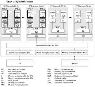
1. 就硬體上來看,一個相容 CBEA 的處理器可由以下幾種方式來組成:
a. a single-chip
b. multi-chip module (or modules)
c. multiple single-chip modules on a mother board
d. second-level package
〔一句話,讚到沒話說,果然是搞超級電腦的IBM啊~〕
2. 就邏輯上來看,CBEA 定義了下列四種 functional components
a. PowerPC Processor Element(PPE)
b. Synergistic Processor Unit (SPU)
c. Memory Flow Controller (MFC)
d. Internal Interrupt Controller (IIC).
3. 每一個 SPU 需要一個對應的 Local Store, 一個 MFC 來指定其 MMU與 Replacement Management Table (RMT)。這樣的組合就稱為 SPU Element (= SPE)。
〔原來這才是 SPE 的定義啊!網路文件果然不完整令人誤會~〕
4. CBEA-Compliant Processor
• One or more PowerPC Processor Elements (PPEs)
• One or more Synergistic Processor Elements (SPEs), which are the combination of a Synergistic Processor Units (SPUs), a local storage area, and a Memory Flow Controller (MFC)
• One Internal Interrupt Controller (IIC)
• One Element Interconnect Bus (EIB) for connecting units within the processor
5. A primary function of the PPEs is the management and allocation of tasks for the SPEs in a system.
〔PPE 的主要功能是管理 SPEs 的 Tasks〕
6. SPU have a single instruction, multiple data (SIMD) capability and typically process data and initiate any required data transfers (subject to access properties set up by a PPE) in order to perform their allocated tasks.
〔SPU 具有 SIMD 能力,並能要求傳輸資料的要求以完成被指定的工作。〕
7. The purpose of the SPU is to enable applications that require a higher computational unit density and can effectively use the provided instruction set.
〔SPU 的主要目的是讓需要高度運算的程式能有效的使用它的指令集。〕
8. MFC components are essentially the data transfer engines. They provide the primary method for data transfer, protection, and synchronization between main storage and the local storage.
〔MFC 控制 main storage 與 local storage 間的資料傳輸。〕
9. Each MFC can typically support multiple DMA transfers at the same time and can maintain and process multiple MFC commands.
〔每一個 MFC 能同時支援多比 DMA 傳輸,並 maintain 與處理多個MFC Command。〕
10. Each MFC provides one queue for the associated SPU (MFC SPU command queue) and one queue for other processors and devices (MFC proxy command queue).
〔MFC會為各別的元件準備一個 queue,並維護與處理 queue 中的MFC Command。〕
11. Each MFC DMA data transfer command request involves both a local storage address (LSA) and an effective address (EA). The local storage address can directly address only the local storage area of its associated SPU.
〔每一比MFC DMA的資料傳輸都與 local storage address(LSA) 與 effective address(EA)有關。LSA只能指到其 SPU 的 local storage 範圍內。〕
12. An MFC presents two types of interfaces: one to the SPUs and another to all other processors and devices in a processing group.
〔一個 MFC 代表兩種介面,一是 SPU,另一則是其它 processor與 device〕
• SPU Channel: The SPUs use a channel interface to control the MFC. In this case, code running on an SPU can only access the MFC SPU command queue for that SPU.
〔SPU Channel:SPU 使用 channel interface 來控制 MFC。而在 SPU 中的程式僅能存取其 MFC SPU Command queue〕
• Memory-Mapped Register: Other processors and devices control the MFC by using memory-mapped registers. It is possible for any processor and device in the system to control an MFC and to issue MFC proxy command requests on behalf of the SPU.
〔Memory-Mapped Register:代表是由非 SPU 的 processor 與 device 正使用 memory-mapped regisiters 在控制 MFC,並對 SPU 發出 MFC proxy command request。〕
(有夠難翻,大概只有我自己看得懂吧~看不懂的請看原文。)
13. The MFC also supports bandwidth reservation and data synchronization features.
〔太簡單就不翻了。〕
14. The IIC component manages the priority of the interrupts presented to the PPEs. The main purpose of the IIC is to allow interrupts from the other components in the processor to be handled without using the main system interrupt controller.
〔IIC 是由 PPE 來控制的,其主要功能就是代 main system 的 interrupt controller 來代勞。〕
15. In a CBEA-compliant system, software must first check the IIC to determine if the interrupt was sourced from an external system interrupt controller. The IIC is not intended to replace the main system interrupt controller for handling interrupts from all I/O devices.
〔在一個相容 CBEA 的系統中,程式必須先檢查 IIC 來確認 interrupt 是否來自系統之外的 interrupt controller。IIC 並不是用來取代原來 main system 中的 interrupt controller 的。〕
16. Local storage consists of one or more separate areas of memory storage, each one associated with a specific SPU.
〔LS 由一塊或多或分隔的記憶體所組成,而每一塊會對應到一個 SPU。〕
17. Each SPU can only execute instructions (including data load and data store operations) from within its own associated local storage domain.
〔SPU 僅能執行其對應的LSD中的指令。〕
18. Therefore, any required data transfers to, or from, storage elsewhere in a system must always be performed by issuing an MFC DMA command to transfer data between the local storage domain (of the individual SPU) and the main storage domain, unless local storage aliasing is enabled.
〔因此,超出 LS 範圍的資料都必須經由 MFC DMA Command 來要求 MFC 從 main storage domain 中傳入 LS 中,除非 local storage aliasing 被 enabled〕
19. An SPU program references its local storage domain using a local address. However, privileged software can allow the local storage domain of the SPU to be aliased into main storage domain by setting the D bit of the MFC_SR1 to ‘1’. Each local storage area is assigned a real address within the main storage domain. (A real address is either the address of a byte in the system memory, or a byte on an I/O device.) This allows privileged software to map a local storage area into the effective address space of an application to allow DMA transfers between the local storage of one SPU and the local storage of another SPU.
〔一旦 local storage aliasing 被 enabled,每一塊 local storage area 都會被指到 main storage domain。這讓 privileged software 能 map 一塊 local storage area 到某個程式的 effective address,也就允許了 SPU 到其它 SPU 間 local storage 的 DMA 傳輸。〕
20. Data transfers that use the local storage area aliased in the main storage domain should do so as caching inhibited, since these accesses are not coherent with the SPU local storage accesses (that is, SPU load, store, instruction fetch) in its local storage domain. Aliasing the local storage areas into the real address space of the main storage domain allows any other processors or devices, which have access to the main storage area, direct access to local storage. However, since aliased local storage must be treated as noncacheable, transferring a large amount of data using the PPE load and store instructions can result in poor performance. Data transfers between the local storage domain and the main storage domain should use the MFC DMA commands to avoid stalls.
〔重點就是,local storage alias 功能被打開時,是不可使用 cache 的,因為外部的 PPE 或是 device 可由此直接存取 local storage。 SPU 中的程式是 no cache 的設計,所以在沒有 cache 的狀況下最好用 MFC DMA 來存取 local storage ,而非 PPE 的 load/store 指令,就可以避免 PPE stalls。〕
21. Main Storage Addressing 得看 PowerPC Architecture, Book I - III 才能更清楚。應該就是 phsical address, virtual address, segments, pages 等等的東東了。每顆 CPU 實作上都不太相同。
Ch 1.2 Cache Replacement Management Facility
1. Tables for managing TLBs and caches are referred to as replacement management tables (RMTs).
2. An SPE group can also contain an optional cache hierarchy, the SL1 caches, which represent first level caches for DMA transfers.
3. The SL1 caches can also contain an optional RMTs.
Ch 1.3 Instructions, Commands, and Facilities
1. CBEA = Cell Broadband Engine Architecture
2. CBEA supports only big-endian byte ordering.
a. PPE are not required to support little endian.
b. SPUs do not support little endian.
〔這種敘述方法挺怪的,PPE 八成是硬體有支援,但軟體沒驗證,才會這麼敘述吧!〕
3. MFC (Memory Flow Controller) 的 DMA(Direct Memory Access) 指令也不支援 little endian。
〔這...... 很多驅動程式可有得玩了。〕
Ch1 Introduction to Cell Broadband Engine Architecture
1. CBEA 定義的是 a process structure toward distributed processing (分散式運算架構的處理器 - 我自己亂翻的)
2. CBEA 分成兩種環境:
a. User Mode Environment (UME) - For application programmer
b. Privileged Mode Environment (PME) - For software in privileged mode (ex: Operating System)
3. The focus of this document is on the infrastructure around the computational, data movement, communication, synchronization, and resource management components.
* PowerPC Architecture, Books I - III define the PowerPC Processor Element (PPE) components.
* The Synergistic Processor Unit Instruction Set Architecture document defines the Synergistic Processor Unit (SPU) components.
〔這個檔案就 319 頁,不包含上面*的東東,很好很好,有得看了。〕
4. SPU 也可運作在非 CBEA 架構下,只是得自己K SPU Instruction Set 來玩了。
〔這倒是不錯啊~只是凡事都自己來,恐怕死得快!〕
Ch 1.1 Broadband Processor Organization
1. 就硬體上來看,一個相容 CBEA 的處理器可由以下幾種方式來組成:
a. a single-chip
b. multi-chip module (or modules)
c. multiple single-chip modules on a mother board
d. second-level package
〔一句話,讚到沒話說,果然是搞超級電腦的IBM啊~〕
2. 就邏輯上來看,CBEA 定義了下列四種 functional components
a. PowerPC Processor Element(PPE)
b. Synergistic Processor Unit (SPU)
c. Memory Flow Controller (MFC)
d. Internal Interrupt Controller (IIC).
3. 每一個 SPU 需要一個對應的 Local Store, 一個 MFC 來指定其 MMU與 Replacement Management Table (RMT)。這樣的組合就稱為 SPU Element (= SPE)。
〔原來這才是 SPE 的定義啊!網路文件果然不完整令人誤會~〕
4. CBEA-Compliant Processor
• One or more PowerPC Processor Elements (PPEs)
• One or more Synergistic Processor Elements (SPEs), which are the combination of a Synergistic Processor Units (SPUs), a local storage area, and a Memory Flow Controller (MFC)
• One Internal Interrupt Controller (IIC)
• One Element Interconnect Bus (EIB) for connecting units within the processor

5. A primary function of the PPEs is the management and allocation of tasks for the SPEs in a system.
〔PPE 的主要功能是管理 SPEs 的 Tasks〕
6. SPU have a single instruction, multiple data (SIMD) capability and typically process data and initiate any required data transfers (subject to access properties set up by a PPE) in order to perform their allocated tasks.
〔SPU 具有 SIMD 能力,並能要求傳輸資料的要求以完成被指定的工作。〕
7. The purpose of the SPU is to enable applications that require a higher computational unit density and can effectively use the provided instruction set.
〔SPU 的主要目的是讓需要高度運算的程式能有效的使用它的指令集。〕
8. MFC components are essentially the data transfer engines. They provide the primary method for data transfer, protection, and synchronization between main storage and the local storage.
〔MFC 控制 main storage 與 local storage 間的資料傳輸。〕
9. Each MFC can typically support multiple DMA transfers at the same time and can maintain and process multiple MFC commands.
〔每一個 MFC 能同時支援多比 DMA 傳輸,並 maintain 與處理多個MFC Command。〕
10. Each MFC provides one queue for the associated SPU (MFC SPU command queue) and one queue for other processors and devices (MFC proxy command queue).
〔MFC會為各別的元件準備一個 queue,並維護與處理 queue 中的MFC Command。〕
11. Each MFC DMA data transfer command request involves both a local storage address (LSA) and an effective address (EA). The local storage address can directly address only the local storage area of its associated SPU.
〔每一比MFC DMA的資料傳輸都與 local storage address(LSA) 與 effective address(EA)有關。LSA只能指到其 SPU 的 local storage 範圍內。〕
12. An MFC presents two types of interfaces: one to the SPUs and another to all other processors and devices in a processing group.
〔一個 MFC 代表兩種介面,一是 SPU,另一則是其它 processor與 device〕
• SPU Channel: The SPUs use a channel interface to control the MFC. In this case, code running on an SPU can only access the MFC SPU command queue for that SPU.
〔SPU Channel:SPU 使用 channel interface 來控制 MFC。而在 SPU 中的程式僅能存取其 MFC SPU Command queue〕
• Memory-Mapped Register: Other processors and devices control the MFC by using memory-mapped registers. It is possible for any processor and device in the system to control an MFC and to issue MFC proxy command requests on behalf of the SPU.
〔Memory-Mapped Register:代表是由非 SPU 的 processor 與 device 正使用 memory-mapped regisiters 在控制 MFC,並對 SPU 發出 MFC proxy command request。〕
(有夠難翻,大概只有我自己看得懂吧~看不懂的請看原文。)
13. The MFC also supports bandwidth reservation and data synchronization features.
〔太簡單就不翻了。〕
14. The IIC component manages the priority of the interrupts presented to the PPEs. The main purpose of the IIC is to allow interrupts from the other components in the processor to be handled without using the main system interrupt controller.
〔IIC 是由 PPE 來控制的,其主要功能就是代 main system 的 interrupt controller 來代勞。〕
15. In a CBEA-compliant system, software must first check the IIC to determine if the interrupt was sourced from an external system interrupt controller. The IIC is not intended to replace the main system interrupt controller for handling interrupts from all I/O devices.
〔在一個相容 CBEA 的系統中,程式必須先檢查 IIC 來確認 interrupt 是否來自系統之外的 interrupt controller。IIC 並不是用來取代原來 main system 中的 interrupt controller 的。〕
16. Local storage consists of one or more separate areas of memory storage, each one associated with a specific SPU.
〔LS 由一塊或多或分隔的記憶體所組成,而每一塊會對應到一個 SPU。〕
17. Each SPU can only execute instructions (including data load and data store operations) from within its own associated local storage domain.
〔SPU 僅能執行其對應的LSD中的指令。〕
18. Therefore, any required data transfers to, or from, storage elsewhere in a system must always be performed by issuing an MFC DMA command to transfer data between the local storage domain (of the individual SPU) and the main storage domain, unless local storage aliasing is enabled.
〔因此,超出 LS 範圍的資料都必須經由 MFC DMA Command 來要求 MFC 從 main storage domain 中傳入 LS 中,除非 local storage aliasing 被 enabled〕
19. An SPU program references its local storage domain using a local address. However, privileged software can allow the local storage domain of the SPU to be aliased into main storage domain by setting the D bit of the MFC_SR1 to ‘1’. Each local storage area is assigned a real address within the main storage domain. (A real address is either the address of a byte in the system memory, or a byte on an I/O device.) This allows privileged software to map a local storage area into the effective address space of an application to allow DMA transfers between the local storage of one SPU and the local storage of another SPU.
〔一旦 local storage aliasing 被 enabled,每一塊 local storage area 都會被指到 main storage domain。這讓 privileged software 能 map 一塊 local storage area 到某個程式的 effective address,也就允許了 SPU 到其它 SPU 間 local storage 的 DMA 傳輸。〕
20. Data transfers that use the local storage area aliased in the main storage domain should do so as caching inhibited, since these accesses are not coherent with the SPU local storage accesses (that is, SPU load, store, instruction fetch) in its local storage domain. Aliasing the local storage areas into the real address space of the main storage domain allows any other processors or devices, which have access to the main storage area, direct access to local storage. However, since aliased local storage must be treated as noncacheable, transferring a large amount of data using the PPE load and store instructions can result in poor performance. Data transfers between the local storage domain and the main storage domain should use the MFC DMA commands to avoid stalls.
〔重點就是,local storage alias 功能被打開時,是不可使用 cache 的,因為外部的 PPE 或是 device 可由此直接存取 local storage。 SPU 中的程式是 no cache 的設計,所以在沒有 cache 的狀況下最好用 MFC DMA 來存取 local storage ,而非 PPE 的 load/store 指令,就可以避免 PPE stalls。〕
21. Main Storage Addressing 得看 PowerPC Architecture, Book I - III 才能更清楚。應該就是 phsical address, virtual address, segments, pages 等等的東東了。每顆 CPU 實作上都不太相同。
Ch 1.2 Cache Replacement Management Facility
1. Tables for managing TLBs and caches are referred to as replacement management tables (RMTs).
2. An SPE group can also contain an optional cache hierarchy, the SL1 caches, which represent first level caches for DMA transfers.
3. The SL1 caches can also contain an optional RMTs.
Ch 1.3 Instructions, Commands, and Facilities
- Instructions define an operation to be performed by a processing element.
- Commands define operations to be performed by the MFC.
- Facilities is a term used to describe functionality accessed through the main storage domain for processors or devices having such access, or by SPUs through the use of channel instructions.
7/14/2006
7/13/2006
7/12/2006
SWF Header Format
Offset                        Value                   Meaning
----------------------------  ---------------------   ----------------------------
0x00                          0x46 = 'F'              Uncompressed
                              0x43 = 'C'              Compressed using ZLIB
                                                      (SWF 6 or later)

0x01                          0x57 = 'W'              Always 'W'

0x02                          0x53 = 'S'              Always 'S'

0x03                          0x06                    Version Number (SWF 6)
                              0x07                    Version Number (SWF 7)

0x04 - 0x07                   FileLength              FWS -> Entire file size in bytes.
                                                      CWS -> Indicate the decompressed file size
                                                             in bytes.


0x08 (bit[7:3])               nBits                   nBits need by the following four field

depend on nBits               Xmin(Signed Integer)    Xmin of Frame Size (Always 0)

depend on nBits               Xmax(Signed Integer)    Xmax of Frame Size

depend on nBits               Ymin(Signed Integer)    Ymin of Frame Size (Always 0)

depend on nBits               Ymax(Signed Integer)    Ymax of Frame Size

After Ymax (2 Bytes)          FrameRate (U16)         Desired playback rate in fps.

After FrameRate (2 Bytes)     FrameCount(U16)         Total number of frames in this SWF.
7/09/2006
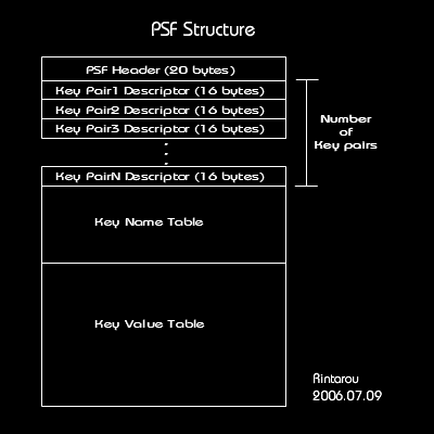
PARAM.SFO Header Format
PARAM.SFO (Space Flight Operations? Similar meanning with what this file for.)

PARAM.SFO 是執行 .PSP 時的各種設定值, 例如: 可執行的地區(Region), 此程式的種類等等
下圖為其主要格式:


PARAM.SFO 是以 Key Name -> Key Value 為一組 Key Pair 的方式來儲存這些設定值的

現在以 2.71 Updater 的 PARAM.SFO 為例子, 來介紹其 Header 格式:

一開始 20 bytes 如下:

00000000h: 00 50 53 46 = .PSF       -> File Identifier
00000004h: 01 01 00 00 = 0x00000101 -> PSF Version Number (Version 5 ?)
00000008h: 44 01 00 00 = 0x00000144 -> Offset of Key Name Table
0000000Ch: f0 01 00 00 = 0x000001f0 -> Offset of Key Value Table
00000010h: 13 00 00 00 = 0x00000013 -> Number of Key Pairs
                               (0x00000013 = 19組 Key)

接著以每16 bytes來描述一組 Key 的實際長度與類別, 所以 19組 Key 共有
304 Bytes(= 19 * 16 Bytes), 下面只介紹第一組為範例說明這 16 Bytes 的定義:

00000014h: 00 00       -> Offset of the Key Name in the Key Table
=> 第一組 Key 的 Key Name 是從 Key Name Table 的第 0 個 byte 開始
00000016h: 04          -> Unknown, always 4. (Maybe alignment? Or bitmask?)
=> 這個 Byte 可能是為了 Alignment, 但目前都是 4, 但是我個人認為這應該是 bitmask.
00000017h: 04          -> Datatype of the Key Value
=> 0x00 -> Binary data
=> 0x02 -> Text data (UTF-8 string with null-terminated)
=> 0x04 -> Signed Integer data (32bits)
00000018h: 04 00 00 00 -> Length of the Key Value
=> Key Value 的長度, 未加上 padding (in bytes)
0000001Ch: 04 00 00 00 -> Length of (Key Value + Padding)
=> Key Value + Padding 的長度 (in bytes)
00000020h: 00 00 00 00 -> Offset of the Key Value in the Key Value Table
=> 第一組 Key 的 Key Value 是從 Key Value Table 的第 0 個 byte 開始
7/08/2006
PBP Header Format
PBP = Playstation Binary Package?
Use EBOOT.PBP of 2.71 Updater as example:
(All data was saved in Little Endian format)
檔案功能說明:
1. PARAM.SFO
儲存各種 UNKNOWN.PSP 執行時的相關資訊, 例如: UNKNOWN.PSP 為 UMD GAME/UMD Video/UMD Audio/Memeory Stick Game/Wireless Game 等等其中一種, 以及支援何種 Region(地區)等等必要的資訊
2. ICON0.PNG (Thumbnail Icon)
在 PSP 中選擇此 EBOOT.PBP 時, 秀給使用者看的小圖式
3. ICON1.PNG (Movie Icon Highlighted)
4. UNKNOWN.PNG (Thumbnail Icon Highlighted)
5. PIC1.PNG (Background Image)
在 PSP 中選擇此 EBOOT.PBP 時的背景圖
6. SND0.AT3 (Ambient Sound)
在 PSP 中選擇此 EBOOT.PBP 時, 播放的背景音樂
5. UNKNOWN.PSP (PlayStation Program?)
當使用者確定執行此 EBOOT.PBP 時, 所要執行的程式
6. UNKNOWN.PSAR (PlayStation ARchive?)
執行 UNKNOWN.PSP 時, 所需要先載入的 Library?
Use EBOOT.PBP of 2.71 Updater as example:
(All data was saved in Little Endian format)
 00 50 42 50 = 0x50425000 ->  File Identifier

 00 00 01 00 = 0x00010000 ->  Version Number?

 00 00 00 28 = 0x00000028 ->  Offset of PARAM.SFO

 48 08 00 00 = 0x00000848 ->  Offset of ICON0.PNG

 45 34 00 00 = 0x00003445 ->  Offset of ICON1.PMF

 45 34 00 00 = 0x00003445 ->  Offset of UNKNOWN.PNG

 45 34 00 00 = 0x00003445 ->  Offset of PIC1.PNG

 45 34 00 00 = 0x00003445 ->  Offset of SND0.AT3

 45 34 00 00 = 0x00003445 ->  Offset of UNKNOWN.PSP

 85 DB 4D 00 = 0x004DDB85 ->  Offset of UNKNOWN.PSAR
檔案功能說明:
1. PARAM.SFO
儲存各種 UNKNOWN.PSP 執行時的相關資訊, 例如: UNKNOWN.PSP 為 UMD GAME/UMD Video/UMD Audio/Memeory Stick Game/Wireless Game 等等其中一種, 以及支援何種 Region(地區)等等必要的資訊
2. ICON0.PNG (Thumbnail Icon)
在 PSP 中選擇此 EBOOT.PBP 時, 秀給使用者看的小圖式
3. ICON1.PNG (Movie Icon Highlighted)
4. UNKNOWN.PNG (Thumbnail Icon Highlighted)
5. PIC1.PNG (Background Image)
在 PSP 中選擇此 EBOOT.PBP 時的背景圖
6. SND0.AT3 (Ambient Sound)
在 PSP 中選擇此 EBOOT.PBP 時, 播放的背景音樂
5. UNKNOWN.PSP (PlayStation Program?)
當使用者確定執行此 EBOOT.PBP 時, 所要執行的程式
6. UNKNOWN.PSAR (PlayStation ARchive?)
執行 UNKNOWN.PSP 時, 所需要先載入的 Library?
7/05/2006
FAT12 Document
PSP is using FAT12 as the file system of flash0 and flash1.
http://www.mega-tokyo.com/osfaq/FAT12%20document
http://www.mega-tokyo.com/osfaq/FAT12%20document
7/04/2006
K5E5658HCM-D060 Note
1 Page    = 512 Bytes(Data) + 16 Bytes(Spare Area)

1 Block   = 32 Pages
          = 16 KBytes(Data) + 512 Bytes (= 32 * 16 Bytes) (Spare Area)

1 Device  = 2048 Blocks
          = 64K Pages (= 2048 * 32 Pages)
          = 32 MBytes (= 2048 * 16KBtes) (Data) +
            1 MBytes (= 2048 * 512Bytes) (Spare Area)

A Page can be devided to 1st half page and 2nd half page.
Address Mapping:
A24 - A9 : (16 bits = 2^16 = 64K) Used to address the Page. (= Page Address)
A8 : Used to indicate the 1st half page or 2nd half page. A8 is set to "Low" or "High" by the 00h or 01h Command. (If using word-level addressing, 01h command is not available.)
A0 - A7 : (8 bits = 2^8 = 256), used to address which byte in the half page indicated by A8.
I/O bus : 16 bits bus (Provide byte-level or word-level data transfer/addressing)
Valid Block:
- may include invalid blocks(bad blocks) when first ship.
- The 1st block of the device is guaranteed to be a valid block(16KBytes). No need ECC upto 1K Program/Erase cycles.
- The 2nd and 3rd blocks are good upon shipping.
- Minimun 1004 valid blocks are guaranteed for each continus 128Mb(=16MBytes) memory space. (This seems not so important.)
Misc:
- Read operations are executed in page basis.
- Erase operations are executed in block basis.
- Include one block sized OTP (One Time Programmable).
PSP內部規格簡單的介紹
Brief Introduction of Handheld Game Machine
http://www.inf.ufrgs.br/~rbmotta/Playstation%20Portable%20PSP.ppt
http://www.inf.ufrgs.br/~rbmotta/Playstation%20Portable%20PSP.ppt
7/03/2006
2.5/2.6 Downgrader FINAL Released!
2.5/2.6 Downgrader Final Released
此一版本與 v5 beta 不同之處僅在於會自動偵測系統版本 (2.5/2.6)
消息來源: http://pspupdates.qj.net/2-5-2-6-Downgrader-FINAL-Released-/pg/49/aid/57717
此一版本與 v5 beta 不同之處僅在於會自動偵測系統版本 (2.5/2.6)
消息來源: http://pspupdates.qj.net/2-5-2-6-Downgrader-FINAL-Released-/pg/49/aid/57717
7/02/2006
1.5 Helper 程式分析
程式運作原理:
1. 建立 ms0:/DOWNDATER/ 目錄結構, 用以存放 downgrader v5 beta 所需要的程式及檔案.
目錄建立結構如下:
sceIoMkdir("ms0:/DOWNDATER", 0777);
sceIoMkdir("ms0:/DOWNDATER/PRX", 0777);
sceIoMkdir("ms0:/DOWNDATER/DUMP", 0777);
sceIoMkdir("ms0:/DOWNDATER/DUMP/data", 0777);
sceIoMkdir("ms0:/DOWNDATER/DUMP/data/cert", 0777);
sceIoMkdir("ms0:/DOWNDATER/DUMP/dic", 0777);
sceIoMkdir("ms0:/DOWNDATER/DUMP/font", 0777);
sceIoMkdir("ms0:/DOWNDATER/DUMP/kd", 0777);
sceIoMkdir("ms0:/DOWNDATER/DUMP/kd/resource", 0777);
sceIoMkdir("ms0:/DOWNDATER/DUMP/vsh", 0777);
sceIoMkdir("ms0:/DOWNDATER/DUMP/vsh/etc", 0777);
sceIoMkdir("ms0:/DOWNDATER/DUMP/vsh/module", 0777);
sceIoMkdir("ms0:/DOWNDATER/DUMP/vsh/resource", 0777);
2. 將 1.5 updater 中的重要相關程式讀出後寫入 ms0:/DOWNDATER/PRX/目錄中, 以提供 downgrader v5 beta 來使用, 其中重要的程式如下
"ms0:/DOWNDATER/PRX/libpsar.prx",
"ms0:/DOWNDATER/PRX/chkuppkg.prx",
"ms0:/DOWNDATER/PRX/lflash_fatfmt.prx",
"ms0:/DOWNDATER/PRX/testmode.prx",
"ms0:/DOWNDATER/PRX/lepton_update.prx",
"ms0:/DOWNDATER/PRX/ipl_update.prx",
"ms0:/DOWNDATER/PRX/suspend_canceler.prx"
3. 將目前 1.5 版 flash0 中的所有目錄及檔案複製到 ms0:/DOWNDATER/DUMP/目錄中, 以提供
downgrader v5 beta 用以取代 2.5/2.6 版的 flah0
(flash0 : 為 kernel mode access only 的 FAT12 partition)
4. 完成 ms0:/DOWNDATER/
PSP 2.6 -> 1.5 降本程式發佈了
http://pspupdates.qj.net/-Breaking-News-2-50-2-60-Downgrader-v5-Beta-Released/pg/49/aid/57594
訂閱:
文章 (Atom)